Thin Film Deposition
An essential building block of MEMS processing
Teledyne MEMS has the ability to deposit thin films of material according device requirements range from a few hundred angstroms to tens of microns or more.
Expansive range of thin films for MEMS sensors
High-quality thin-film deposition can enhance performance and improve yields, but a larger variety of thin films are required for MEMS sensors. Teledyne MEMS offers the films and fabrication techniques required to produce high quality electrodes that can be paired to deliver consistent results.
Teledyne MEMS uses various techniques for thin film deposition including sputtering and evaporation. After the film is successfully deposited, it is ready for photolithography or other wafer etching methods.
Sputtering
Consistent film quality across layers
Custom thin film metallization consists of sputtering metal coatings with patterns made to customer specifications. Our engineers use multi-target sputtering systems to provide consistent film quality and access to custom adhesion, barrier, conductive and electrode layers, as well as serving in a number of other functions unique to MEMS processing.
Depending on the material selected, thin film sputtered layers can range from 5 nm for adhesion layers to microns for conduction layers. Patterning is done to match customer specifications using wet chemical etch or liftoff techniques.
- Substrates coated: silicon, SOI, glass, quartz, sapphire, diamond, AlN, alumina
- Conductive layers: gold (Au), copper (Cu), aluminum (Al)
- Barrier layers: titanium/tungsten (TiW), platinum (Pt), molybdenum (Mo), nickel copper (NiCu)
- Sputtering adhesion layers: chromium (Cr), titanium (Ti), titanium/tungsten (TiW)
- Resistive layers: tantalum nitride (TaN), platinum (Pt)
- Electrode layers: gold (Au), platinum (Pt), silver (Ag)
Nano-Engineered Thin Films
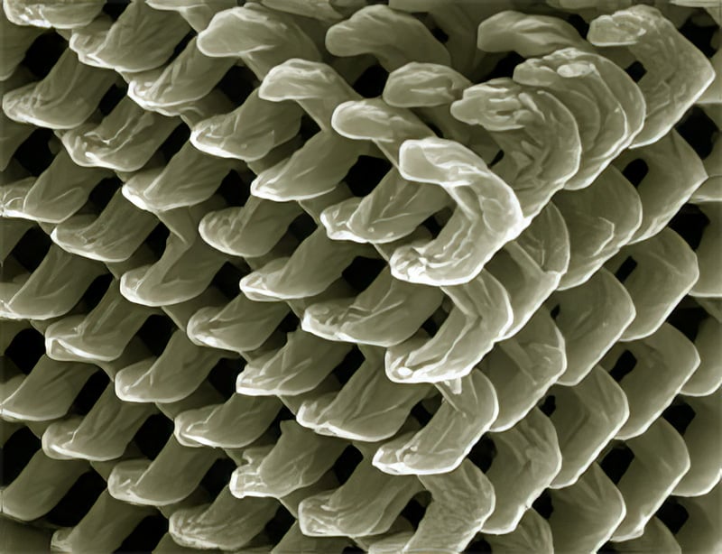
Glancing Angle Deposition (GLAD)
Glancing Angle Deposition (GLAD) for the creation of thin films combines physical vapor deposition with computer-controlled substrate motion to create nano-thin films with engineered nanostructures. These nanostructures can be engineered with features, such as film thickness, porosity, and geometry.
Potential applications of GLAD thin films include:
- High surface electrodes
- Chromatographic media for separations
- Solar cells
- Structural alignment (LCOS, SERS)
- Biosensors for medical diagnostics
- Humidity sensor
- Photonic crystals
GLAD thin films can be engineered to create unique properties for:
- Light manipulation
- Molecular manipulation
- Mechanical response
- Electronic field manipulation
- Protective properties
- Chemical and electrochemical interaction
- Accessible surface area
Chemical Vapor Deposition
Plasma Enhanced Chemical Vapor Deposition (PECVD)
These methods are useful for layer deposition at lower temperatures are needed, such as metal passivation, etch mask generation, sacrificial layer deposition, and mechanical functional layer deposition. Teledyne MEMS has patented unique formulations for PECVD oxynitride film deposited on noble metals used in chemical and biosensors to make superior quality and repeatable electrode surfaces
- PECVD oxide (uniformity < 5%, thickness 100 Å – 7 µm, good stress control)
- PECVD nitride (LF/HF) (uniformity < 5%, stress control ± 50 MPa)
- PECVD oxynitride
- PECVD amorphous silicon
- LPCVD polysilicon
Electron-Beam Evaporation
Extreme precision across complex surfaces
This thin film deposition technique involves a highly-focused electron beam directed toward a high purity source material in a high vacuum chamber at room temperature. The source material is evaporated and then condenses on all exposed cool surfaces on the vacuum chamber and substrate. The process is typically performed on one side of the substrate at a time, allowing the ability to rotate several source materials into the path of the electron beam, depositing multiple thin films sequentially without breaking vacuum.
- Liftoff compatible processes, < 5% uniformity)
- Al, Ag, Au, Cr, Ni, Pt, SiO2, Ti
- Thickness: 100 Å – 2 µm
Teledyne MEMS Capabilities
We blend MEMS applications experts together with process performance champions to design process flows for robust, cost-effective fabrication to match customer requirements. Our project teams strive for deep insights to their customers’ needs and close communications throughout the relationship.

Do you have any questions?
Select Teledyne as your partner to move your MEMS device from concept to mass production.
Contact usStay connected
The MEMS industry is evolving quickly with new innovations, applications, and events. Subscribe to our newsletter and we’ll help you keep up to date with the latest developments
Subscribe